Copper
Interconnects

Interconnects
Features
Identifying critical defects in copper
Our AI provides solutions
Train a pipeline specific to your defects.
Autofocus
Advanced autofocus algorithms determine an autofocus map to deliver precise results across batches.
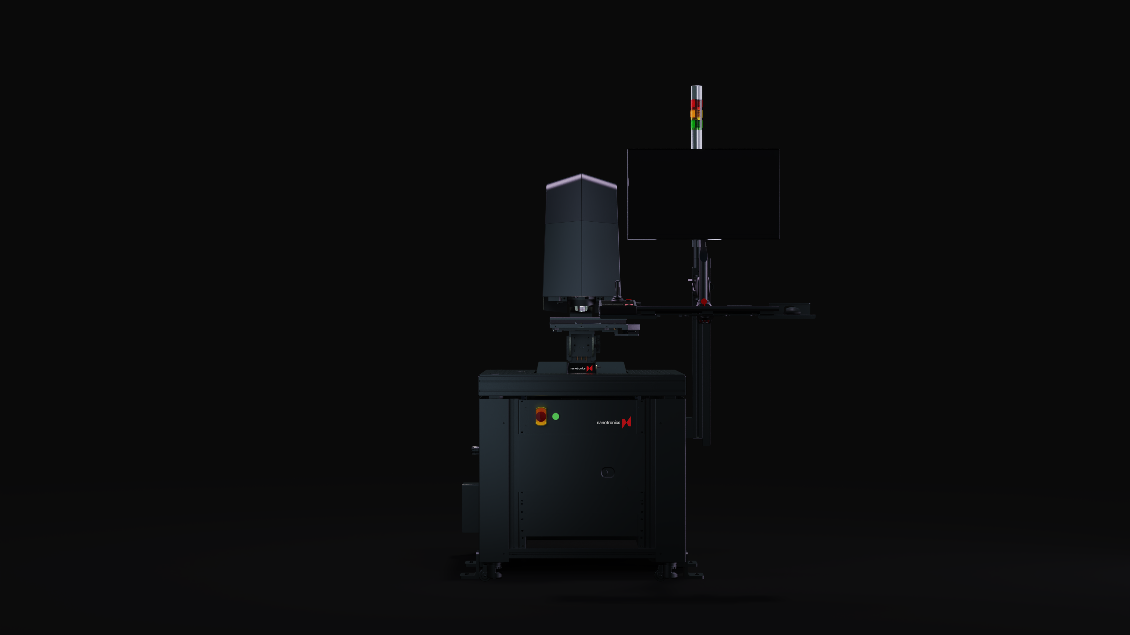
Recommended Product
nSpecLS
The nSpec LS can efficiently increase yields in the lab and scale processes.
System highlights
ModularField upgradeable to automated system
Max wafer size300 mm
Scan resolution0.9 µm/pixel (w/ 5x objective)

Benefits
Defect types
Surface roughness
Determine surface roughness or haze to prevent non-uniform surfaces in subsequent processing steps.
Industries
Our solutions are tailored to meet the unique challenges and demands of each sector.
Downloads
Contact Us