Silicon
Microprocessors

Microprocessors
Identifying critical defects in silicon
Our AI provides solutions
Train a pipeline specific to your defects.
Identify micropits and basal plane defects
Analyzers tuned for precise classification of different defects.
Recommended Product
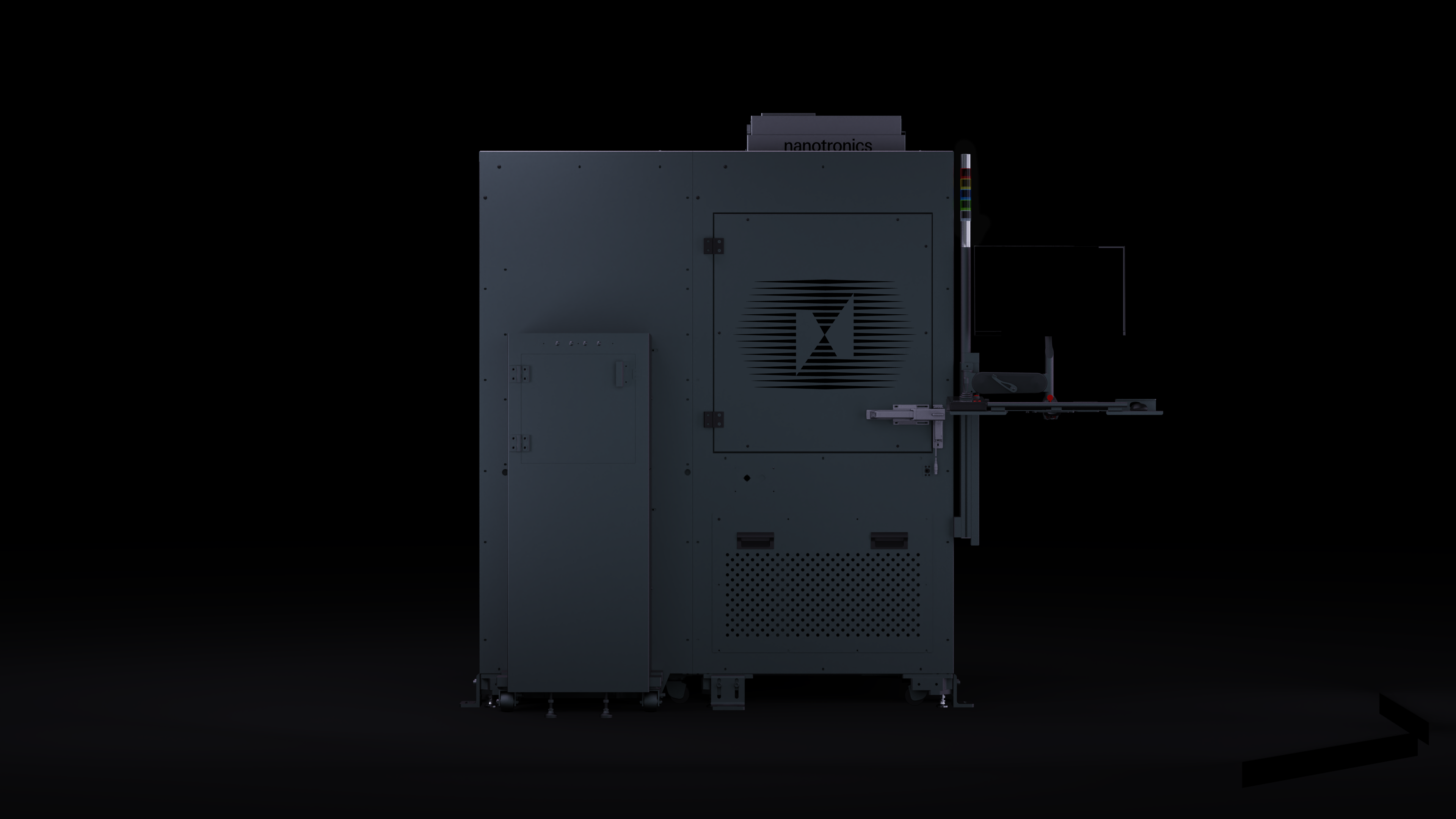
nSpecTURBO
The nSpec TURBO is the ideal system for fully automated high volume manufacturing environments.
System highlights

Defect types
Crystalline dislocations
Identify lattice mismatch to prevent imperfections in the growth process.
Scratches and micropits
Surface imperfections can affect the quality of subsequent layers deposited on the wafer.
Bow and warp
Measure bow and warp to ensure a perfectly flat surface before lithography and patterning processes.
Foreign material contamination
Identify small particles from equipment or the environment during processing.
Gallium Nitride on Silicon
Grow gallium nitride on silicon substrate.
Dislocations
On etched wafers, detect defect types by shape and provide counts, sizes, and locations for all defects, such as threading edge dislocations and threading screw dislocations.
V-pit or inverted pyramids
Identify defects that will cause voltage leaks.
Lattice mismatch
Easily identify lattice mismatch and thermal stress from a difference in thermal expansion coefficients.
Foreign material contamination
Identify small particles from equipment or the environment during processing.