Epitaxial Wafers

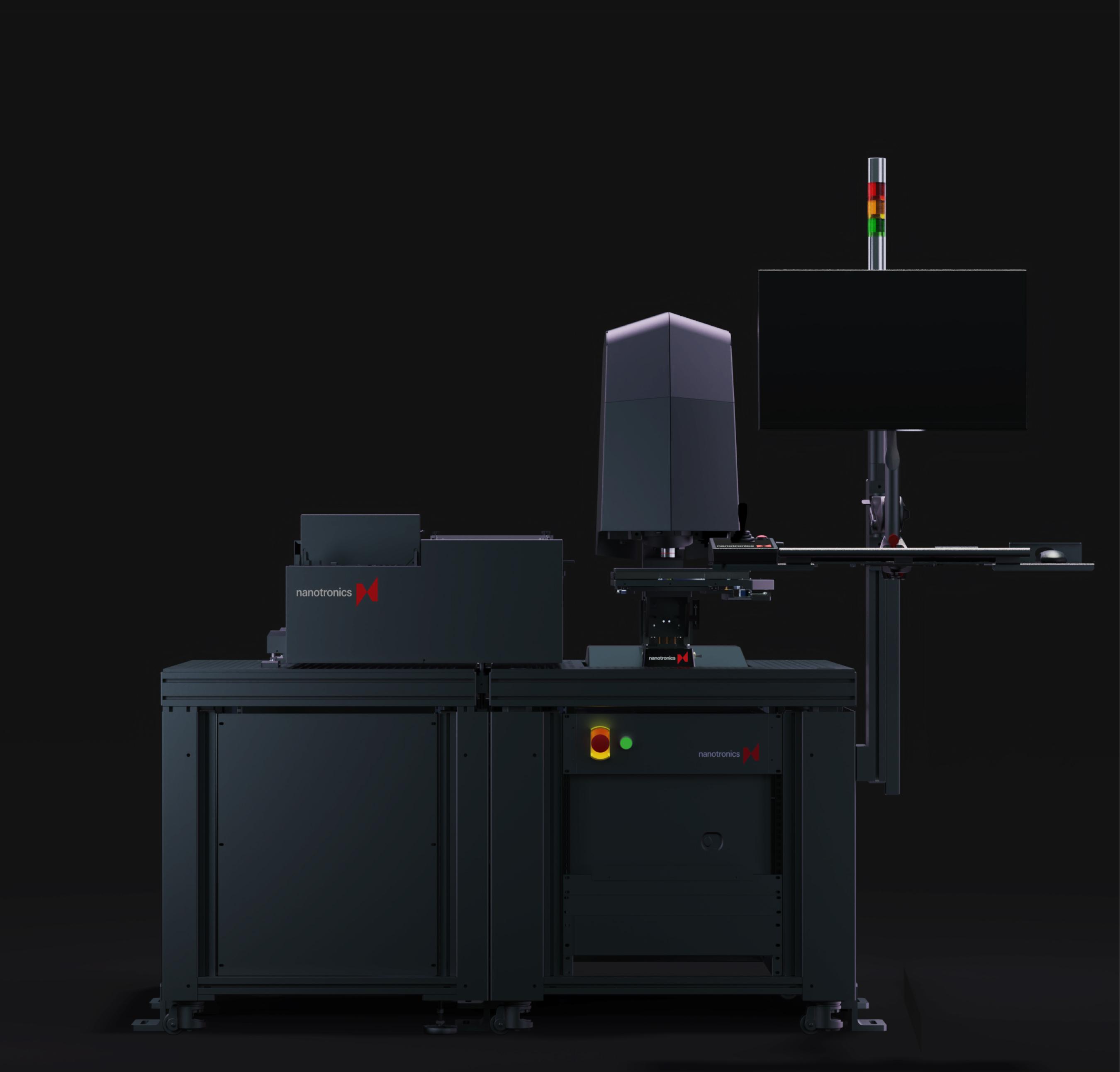
Perform rapid, full-sample defect detection and classification on epitaxial wafers.

Benefits

Non-destructive defect detection

Detect dislocations, slip line defects, and crack defects without destructive etching methods.

AI-powered defect classification

Quickly classify and distinguish between epitaxial and substrate defects using nTelligence.

Flexible output formats

Export defect data using industry-standard formats.

Recommended Product

nSpecPS

The nSpec PS is highly flexible and detects defects in a variety of wafers, substrates, and materials.

Learn more
Automated optical inspection tool with robotic wafer loader, nSpec PS
Industries

Our solutions are tailored to meet the unique challenges and demands of each sector.

Resources

More helpful resources from Nanotronics

Insights

Is Artificial Intelligence Cost-Effective? 16 Ways AI Helps Companies Save Money

Read More
Overhead view of three coworkers, two men and one woman, at an office table going over blueprints and plans
Insights

Identifying Where to Apply Machine Learning in Manufacturing

Read More
Modern High Tech Authentic Robot Arm Holding Contemporary Super Computer Processor. Industrial Robotic Manipulator End Effector Holding CPU Chip
Contact Us

Get in touch with one of our industry experts.

Let's talk logistics.

Let’s talk about how Nanotronics can transform your manufacturing process.
Contact Us

Free sample report

Having trouble classifying critical defects? Nanotronics can help.
Get Sample Report