Sapphire
LEDs

LEDs
Identifying critical defects in sapphire
Autofocus
Advanced autofocus algorithms determine an autofocus map to deliver precise results across batches.
Golden template
nSpec generates a golden template to compare against scan images. To ignore feature boundaries, fiducial marks, and other regions, a mask is applied to the golden template.
Recommended Product
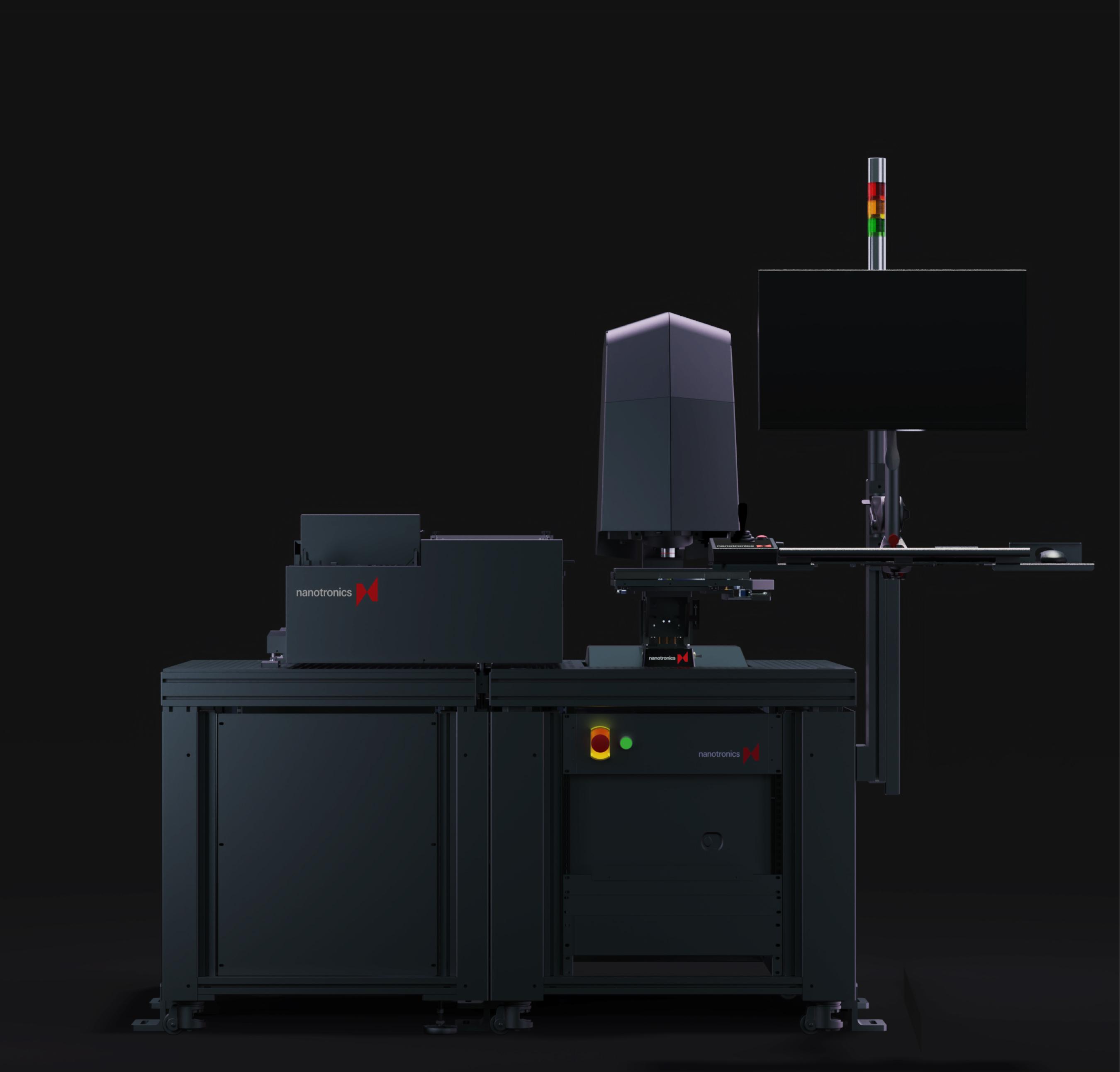
nSpecPS
The nSpec PS is highly flexible and detects defects in a variety of wafers, substrates, and materials.
System highlights

Defect types
Craters
Determine irregularities that occur during the plating process.
Pillars
Pillar defects can affect device performance, reliability, and yield.
Stains
Identify color differences during fabrication process to prevent degraded electrical properties.
Silicon on Sapphire
Grow silicon epitaxy on sapphire substrate.
Dislocations
On etched wafers, detect defect types by shape and provide counts, sizes, and locations for all defects, such as threading edge dislocations, and threading screw dislocations.
Lattice mismatch
Easily identify lattice mismatch and thermal stress from a difference in thermal expansion coefficients.
Surface roughness
Determine surface roughness or haze to prevent non-uniform surfaces in subsequent processing steps.