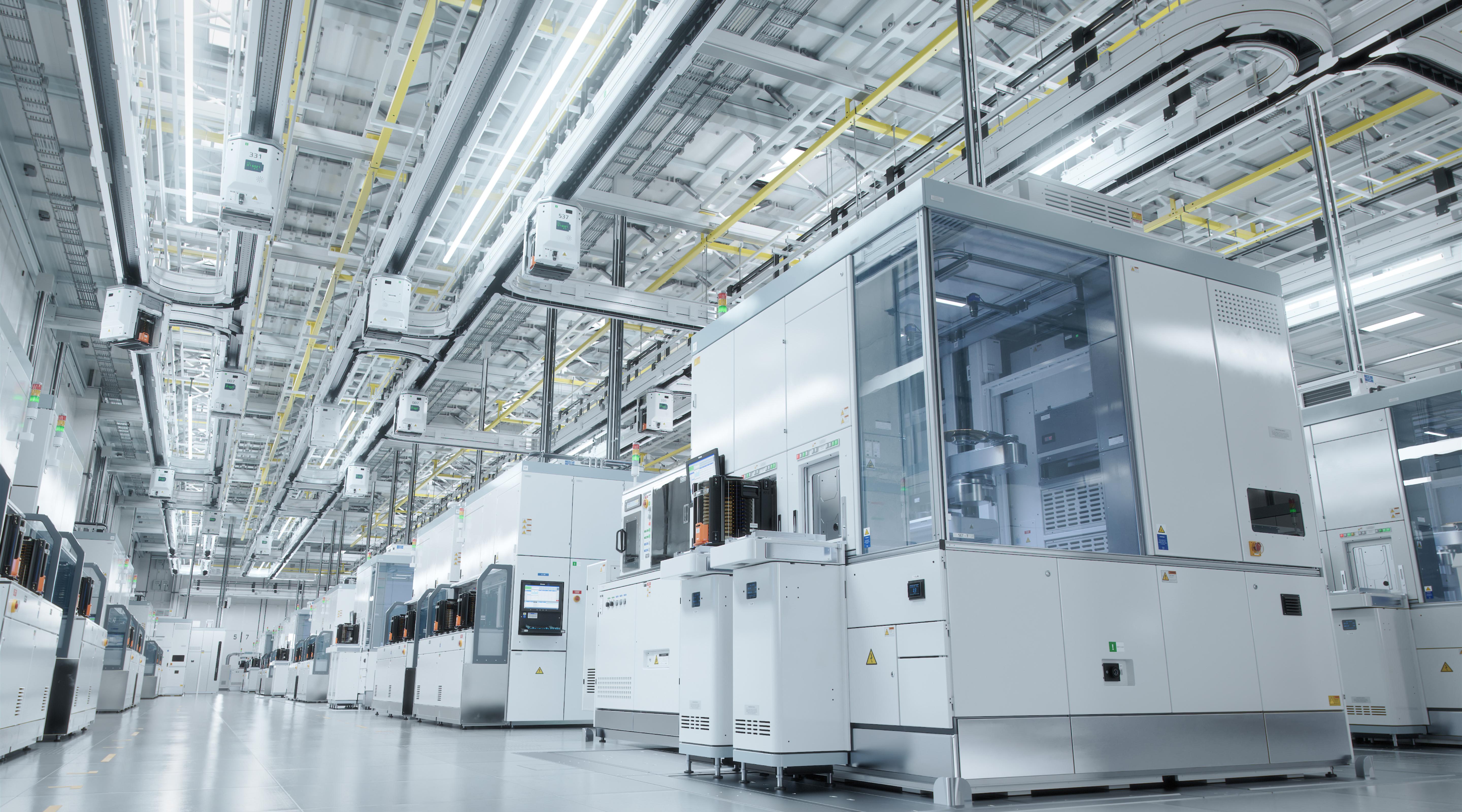
Semiconductors
Transforming our information infrastructure, down to the nanoscale

Drive chip yields higher
Semiconductors are the foundation of the modern world — from communications technology to flight controls to medical devices. Nanotronics’ advanced systems can be used to ensure quality in any precision process.
Inspection
Our tools are deployed for early detection of microscopic contaminants and manufacturing defects throughout wafer, device, and chip fabrication processes.
Process optimization
Integrating inspection, metrology, and process data, our analysis and process optimization tools use AI to diagnose process problems and drive continuous improvement.

Applications at each stage of the supply chain
Our family of inspection and process control tools can be used across semiconductor manufacturing — from substrates through bare and patterned wafers all the way to packaged devices.
Novel materials
Our expertise in compound and wide-bandgap semiconductors gives us a unique edge in applications such as photonics, sensors, wireless devices, and power electronics.
Flexible tools
Our nSpec and nControl inspection and process control tools can be configured for diverse process stages and device designs. Use them across your facilities to gain end-to-end manufacturing insights that scale and adapt along with your processes.