Insights
Is Artificial Intelligence Cost-Effective? 16 Ways AI Helps Companies Save Money

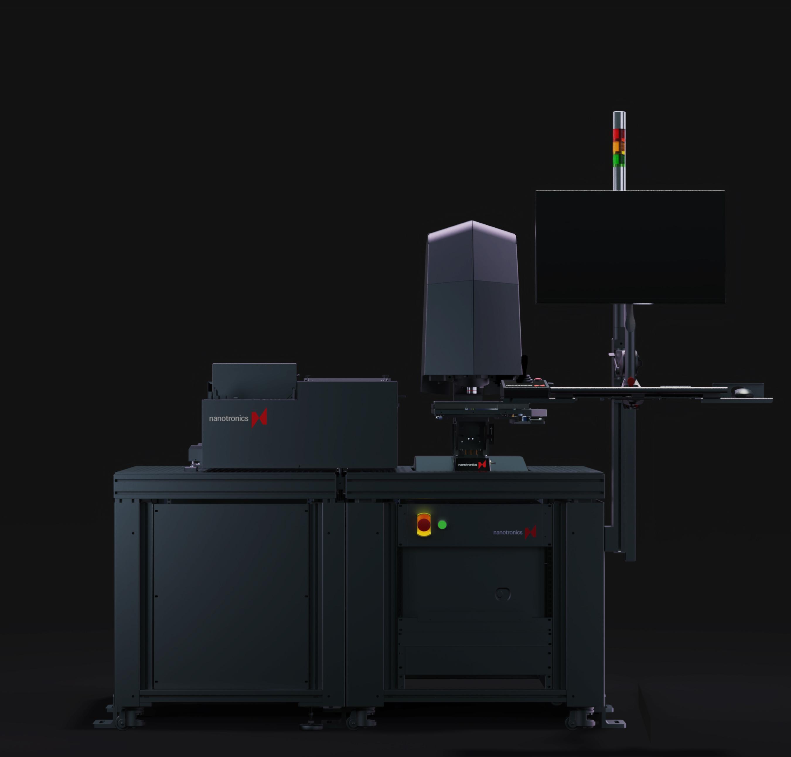
Fully automated frontside and back-side inspection with edge exclusion handling.
Seamlessly handle and inspect samples with multiple sides.
Automatically detect defects in multiple sample planes.
Quickly classify defects with nTelligence.
Maximize device yield calculations with fully customizable parameters, such as region of interest and defect class.
The nSpec PS is highly flexible and detects defects in a variety of wafers, substrates, and materials.
