Photonic Devices

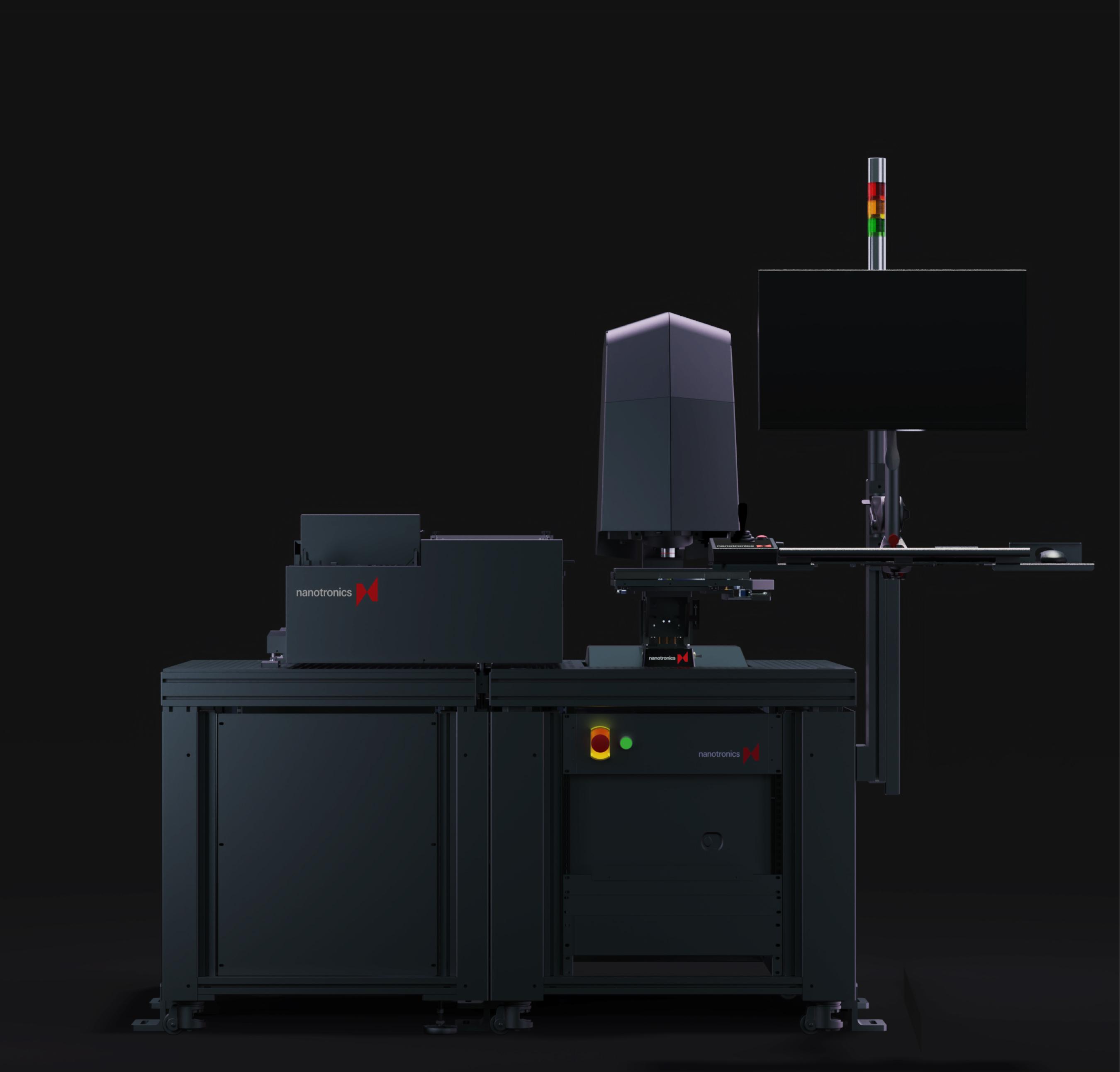
Automated inspection for complex photonic device layouts under high magnification.

Benefits

Maximize device yield

Optimize device yield calculations with fully customizable parameters, such as region of interest and defect class.

Pixel array inspection

Automatically detect defects in pixel arrays at high magnification.

Handle complex layouts

Handles device layouts with complex structures and unusual sizes with ease.

AI-powered defect classification

Quickly classify defects with nTelligence.

Recommended product

nSpecPS

The nSpec PS is highly flexible and detects defects in a variety of wafers, substrates, and materials.

Learn more
Automated optical inspection tool with robotic wafer loader, nSpec PS
Industries

Our solutions are tailored to meet the unique challenges and demands of each sector.

Resources

More helpful resources from Nanotronics

Insights

AI in Manufacturing: 10 Ways AI Is Changing the Manufacturing Industry

Read More
Automatic robots in the industrial factory for assembly automotive products, automotive concept
Insights

A Brief History of Automation in Manufacturing: Then and Now

Read More
Advanced High Precision Robot Arm inside Bright Electronics Factory. Electronic Devices Production Industry. Component Installation on Circuit Board. Fully Automated Modern PCB Assembly Line
Contact Us

Get in touch with one of our industry experts.

Let's talk logistics.

Let’s talk about how Nanotronics can transform your manufacturing process.
Contact Us

Free sample report

Having trouble classifying critical defects? Nanotronics can help.
Get Sample Report