nSpecLS
Learn how the nSpec LS can efficiently increase yields and scale processes

Accelerate research with advanced inspection
Reduce operational costs
nSpec LS allows operators to identify, classify, and assign causality to defects in order to prevent down-line issues.
Increase production output
Early detection allows manufacturers to produce high yields and scale processes quickly.
Speak with one of our product experts
Schedule a personalized demo and learn how Nanotronics can help your operations.
nSpec was purchased in 2013 and is a workhorse for us. It provides invaluable characterization of the properties of every wafer that goes through our facility.
President & CEO
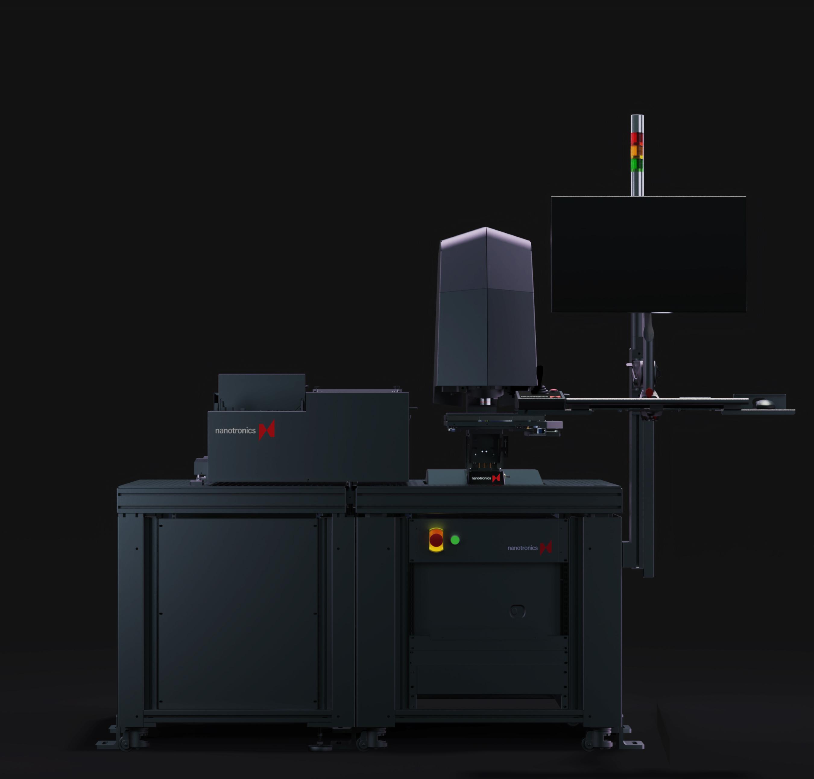
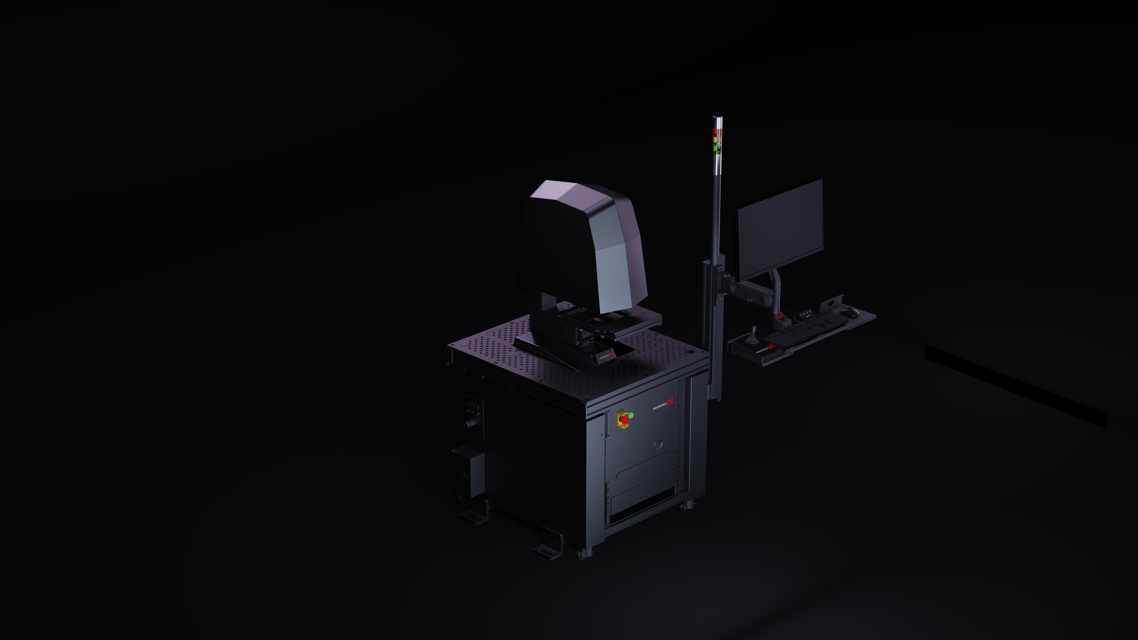
The ideal system for research & development settings
Defect inspection is crucial to scaling next-generation devices. The LS system has a small footprint and is used to identify, classify, and assign causality to defects before you scale to volume production.


Flexible software
User-friendly software makes configuring recipes simple. As needs evolve, recipes are easily saved and modified.


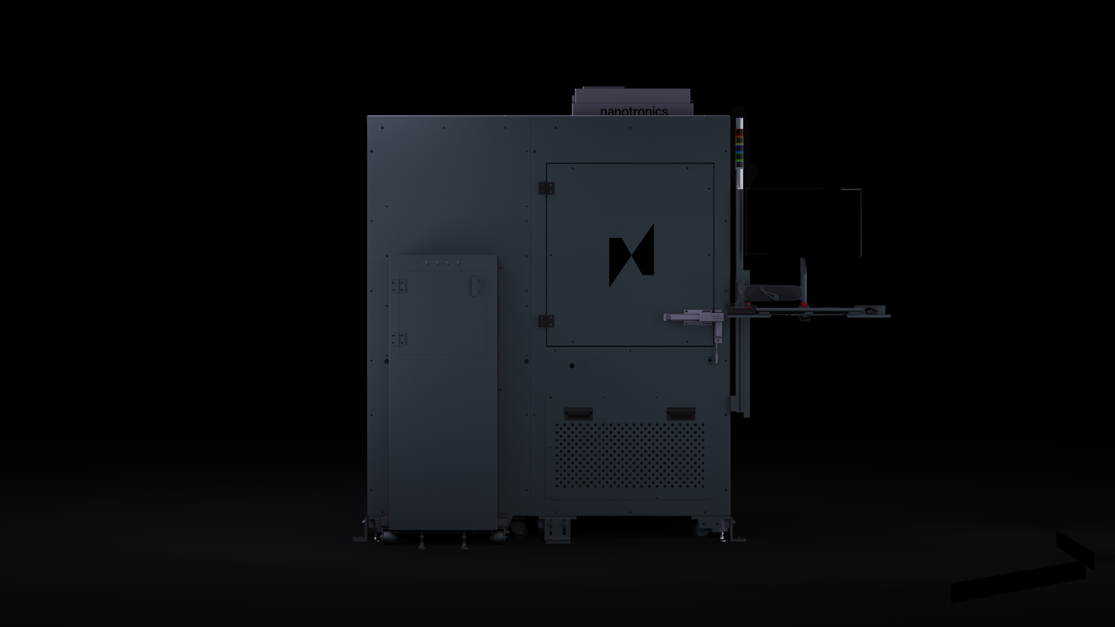
Robust hardware
The nSpec LS can manage various sample form factors and can inspect a wide variety of new and novel materials.


Powered by Nanotronics AI
nTelligence is trained to identify early process defects before scaling to high-volume manufacturing.


Modular design
Easily upgrade the nSpec LS to a PS system when your process is ready to be scaled to volume production.

Find device-killing defects.


System
Weight
240 kg
Dimensions (W x D x H)
165 cm x 157 cm x 194 cm
Min. Vacuum Requirement
-21 in. Hg (-70 kPa)
Power Supply
208—240 VAC, 15A, 50—60 Hz
Optics
Illumination Modes
Brightfield, Darkfield, Automated DIC (Nomarski)
Light Source
White light LED (other options available)
Objectives
5x (included), 1.25x, 2x, 2.5x, 10x, 20x, 50x
Objective Turret
5-position, User‑selectable
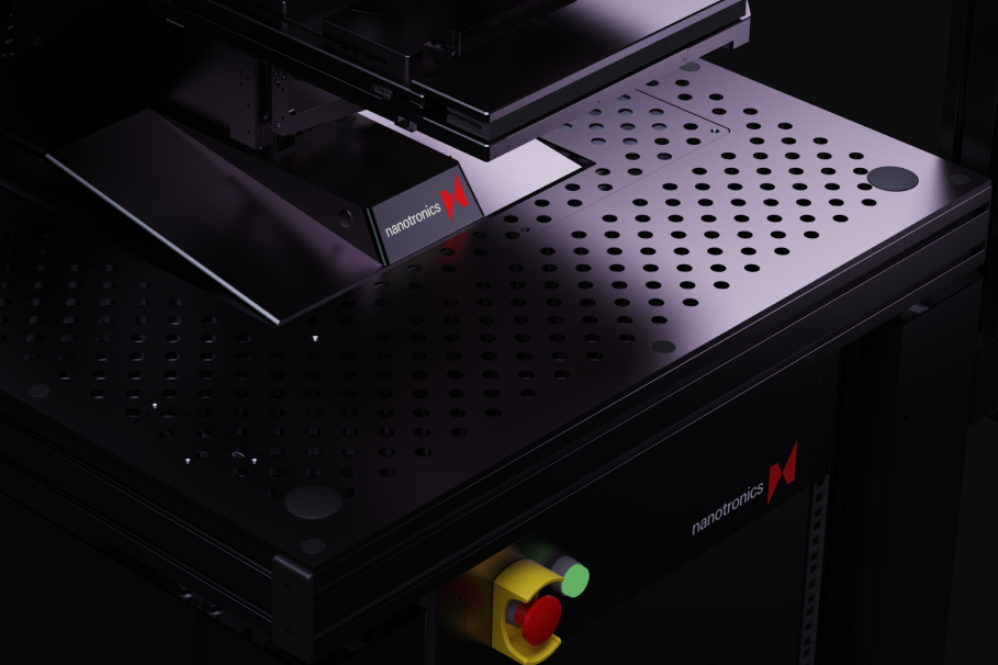
Stage
Travel, typical
200 mm X and Y directions
Positioning
Linear servo motors with closed‑loop encoders (50 nm resolution)
Repeatability
+/- 0.5 µm
Travel Flatness
30 µm
Centered Load Capacity
2.27 kg
Options
Supported Protocols
SECS/GEM
Illumination
Transmitted light with automated polarizer
Filters
12‑position filter wheel
Machine learning
Offline workstation, nTelligence™, Gen‑V‑AI
Automate inspection across your R&D and production lines.
Automated Optical Inspection (AOI) is one of the most efficient forms of device inspection, but it is typically limited by resolution. Nanotronics AI detection algorithms overcome this and detect defects that would otherwise go unnoticed.