Aluminum Nitride
High frequency & high temperature

High frequency & high temperature
Features
Identifying critical defects in aluminum nitride
Handling
nSpec offers flexibility and can handle sample sizes ranging from 50 mm to 300 mm wafers.
Our AI provides solutions
Train a pipeline specific to your defects.
Recommended Product
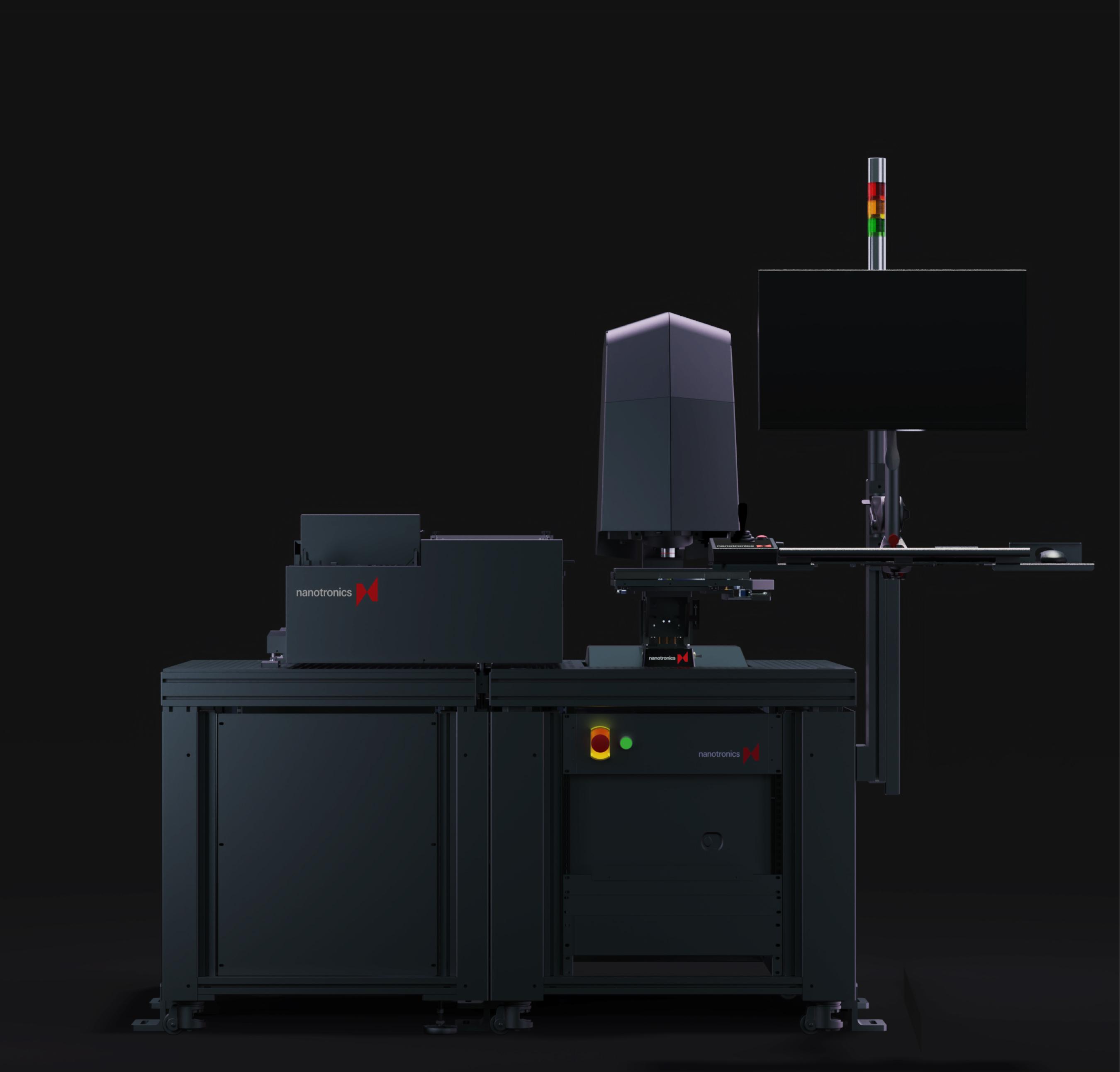
nSpecPS
The nSpec PS is highly flexible and detects defects in a variety of wafers, substrates, and materials.
System highlights
LoadingAutomated wafer loading
Max wafer size200 mm
Scan resolution0.9 µm/pixel (w/ 5x objective)

Benefits
Defect types
Pitting
Classify and quantify pitting defects that can cover the entirety of a wafer.
Planar and void
AI allows operators to classify defects based on size. Planar and void defects generally occupy less surface area.
Industries
Our solutions are tailored to meet the unique challenges and demands of each sector.
Downloads
Contact Us