Insights
6 Key Steps in the Semiconductor Manufacturing Process

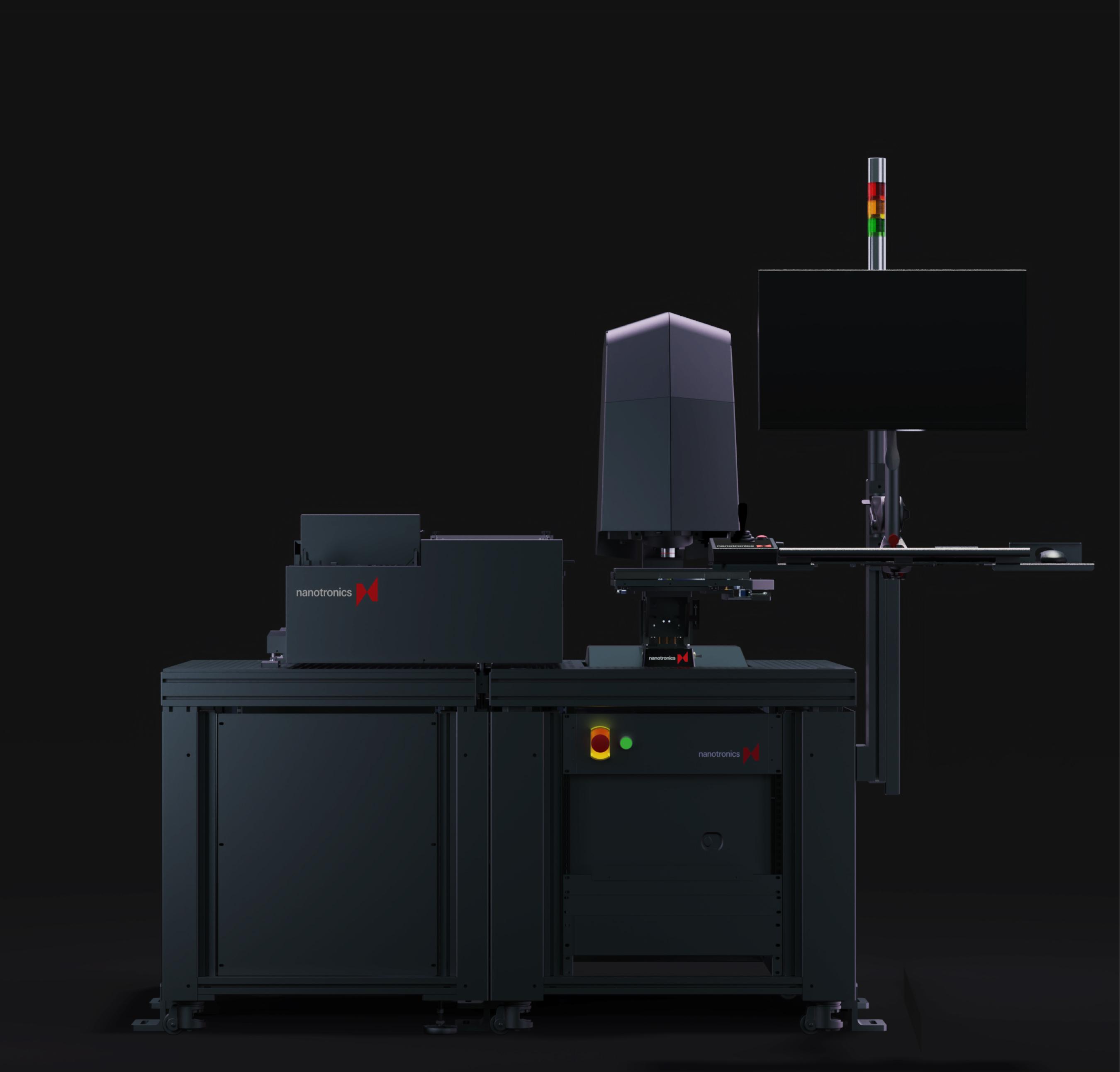
Fully automated inspection throughout all steps of advanced packaging for wafer, panel, substrate or device level.
Automatically load wafers, quarter panels, full panels, and JEDEC trays in one tool.
Quickly classify defects with nTelligence.
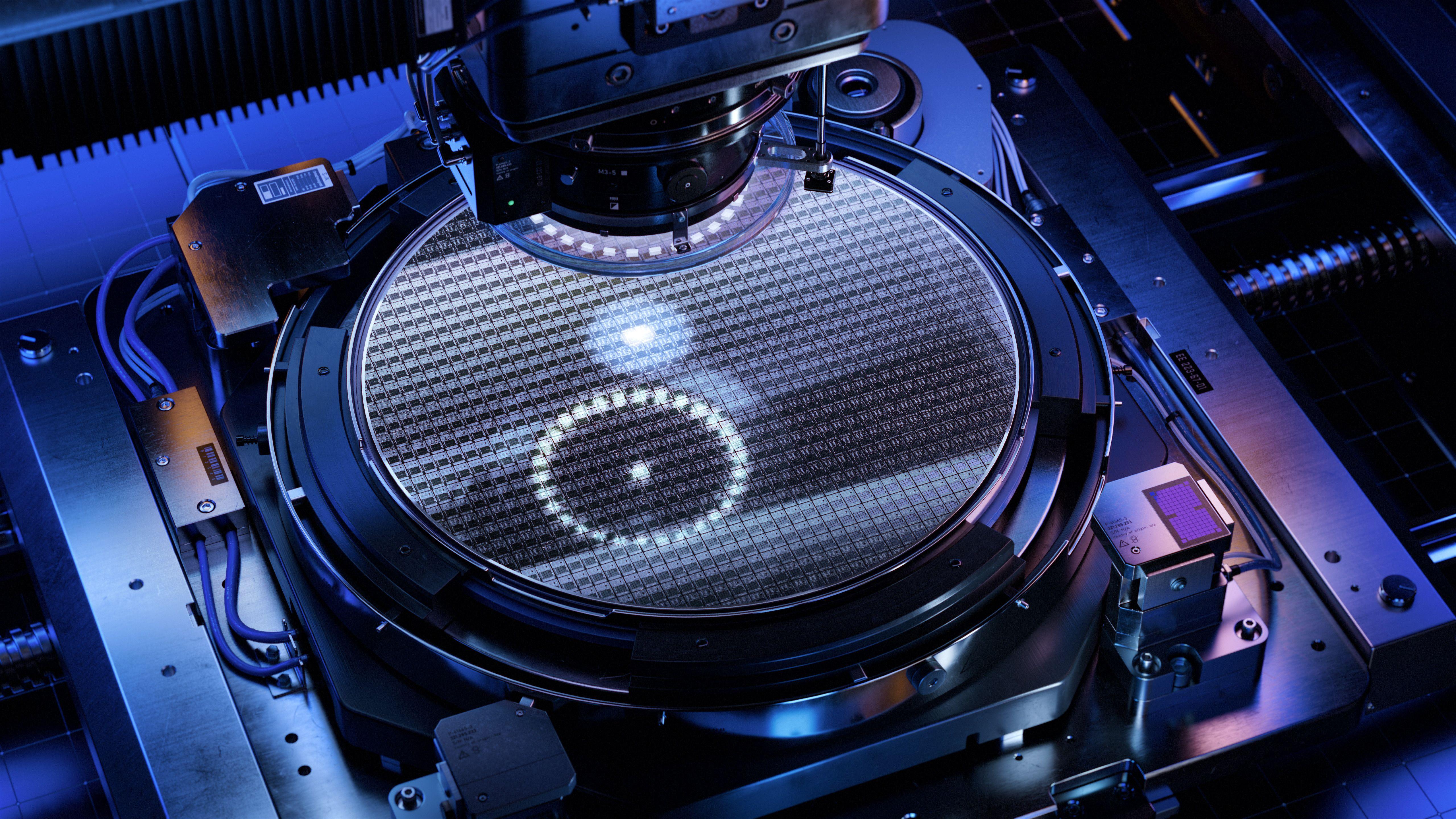
The nSpec PS is highly flexible and detects defects in a variety of wafers, substrates, and materials.