Gallium Nitride
Power electronics

Power electronics
Features
Identifying critical defects in gallium nitride
Our AI provides solutions
Train a pipeline specific to your defects.
Identify micropits and basal plane defects
Analyzers tuned for precise classification of different defects
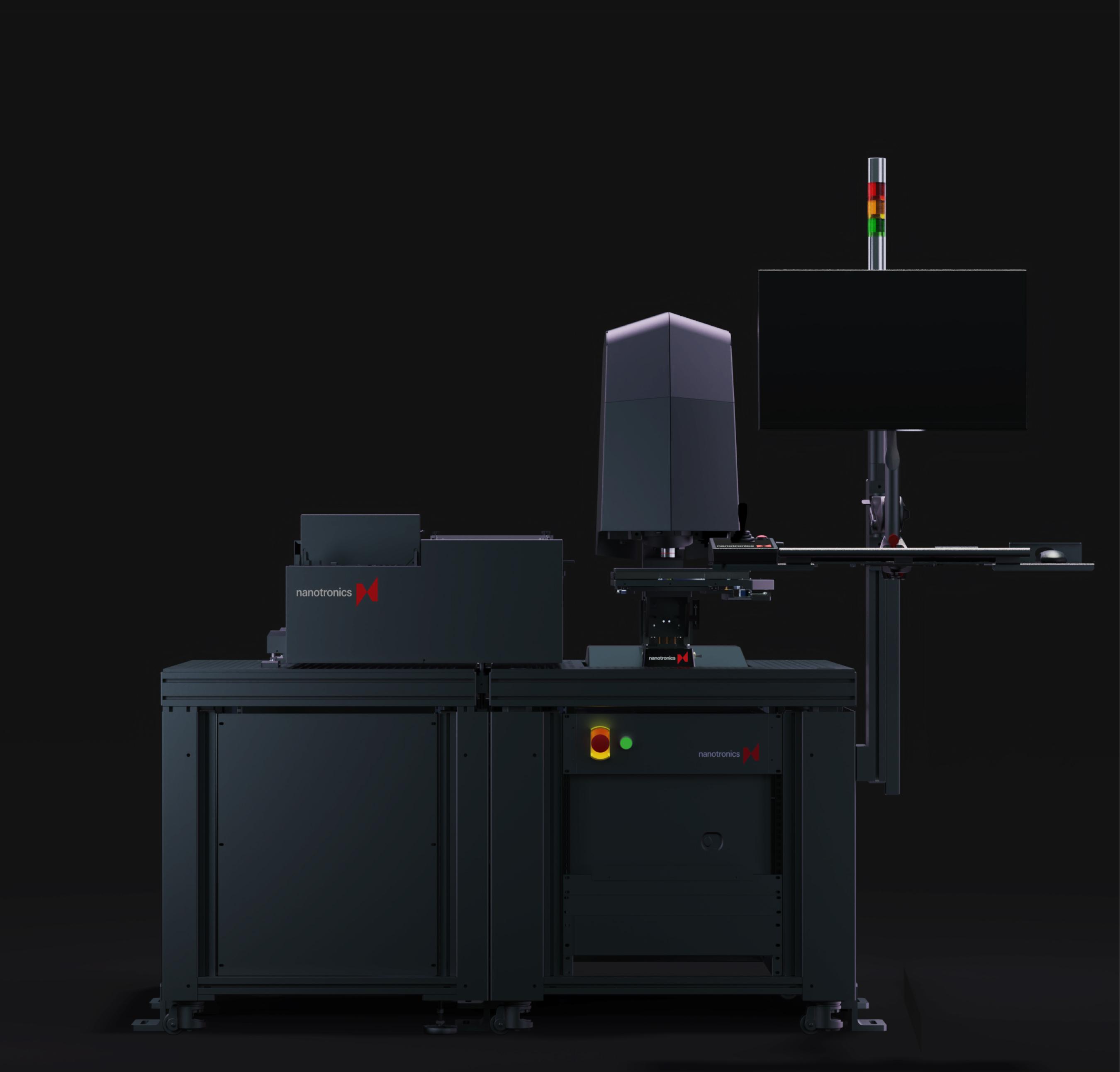
Recommended Product
nSpecPS
The nSpec PS is highly flexible and detects defects in a variety of wafers, substrates, and materials.
System highlights
Loading Automated wafer loading
Max wafer size200 mm
Scan resolution0.9 µm/pixel (w/ 5x objective)

Benefits
Defect types
Dislocations
On etched wafers, detect defect types by shape and provide counts, sizes, and locations for all defects, such as threading edge dislocations and threading screw dislocations.
V-pit or inverted pyramids
Identify defects that will cause voltage leaks.
Lattice mismatch
Easily identify lattice mismatch and thermal stress from a difference in thermal expansion coefficients.
Foreign material contamination
Identify small particles from equipment or the environment during processing.
Industries
Our solutions are tailored to meet the unique challenges and demands of each sector.
Downloads
Contact Us