Insights
What is Wafer-Level Packaging, and What Forms Does it Take?

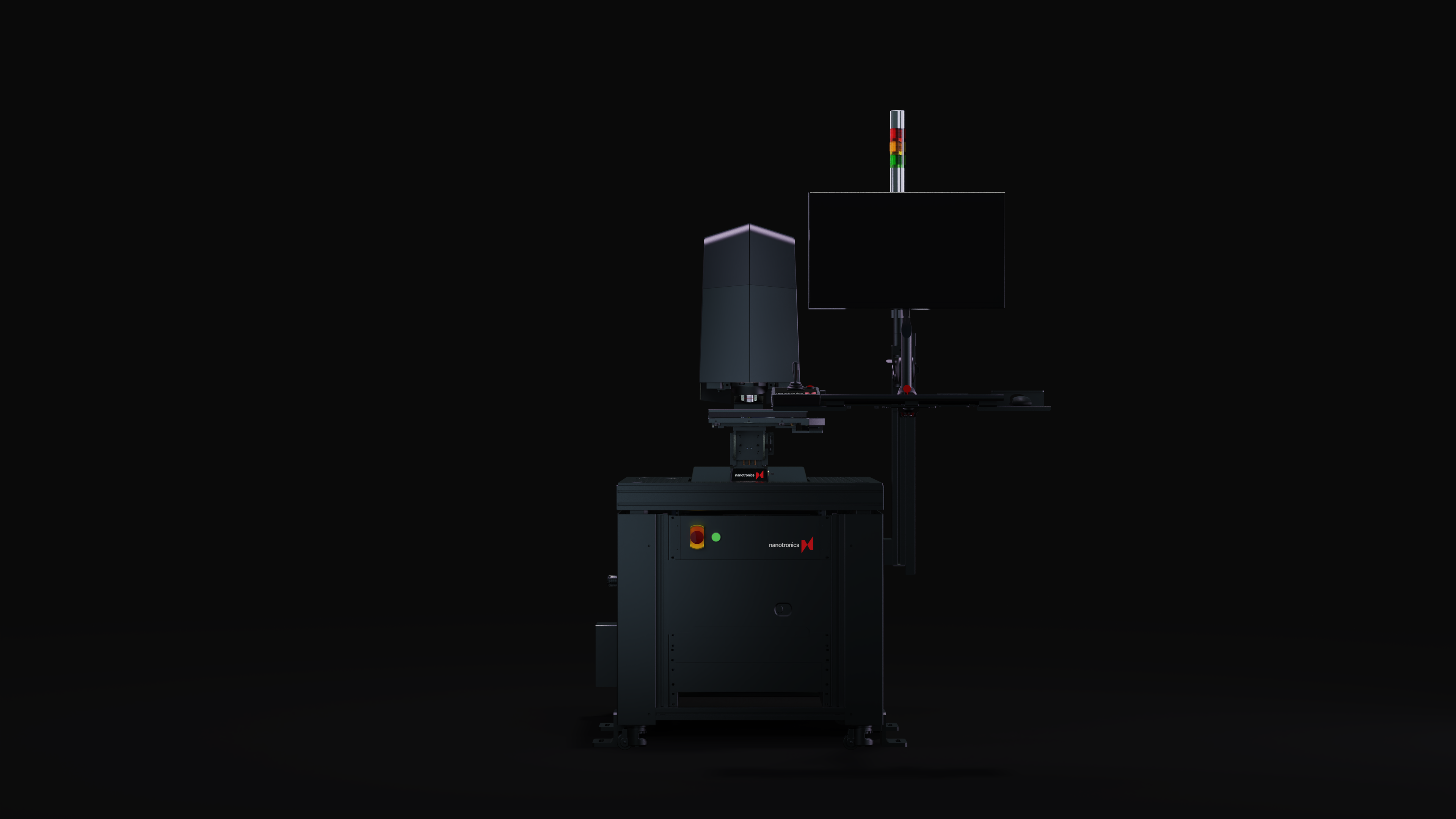
nSpec combines computer vision, AI, optical inspection equipment and advanced robotics to inspect the world’s most sophisticated technologies.
Streamline R&D and improve lab processes for increased yields with precision manufacturing.

Automate inspection from R&D to production with a single tool

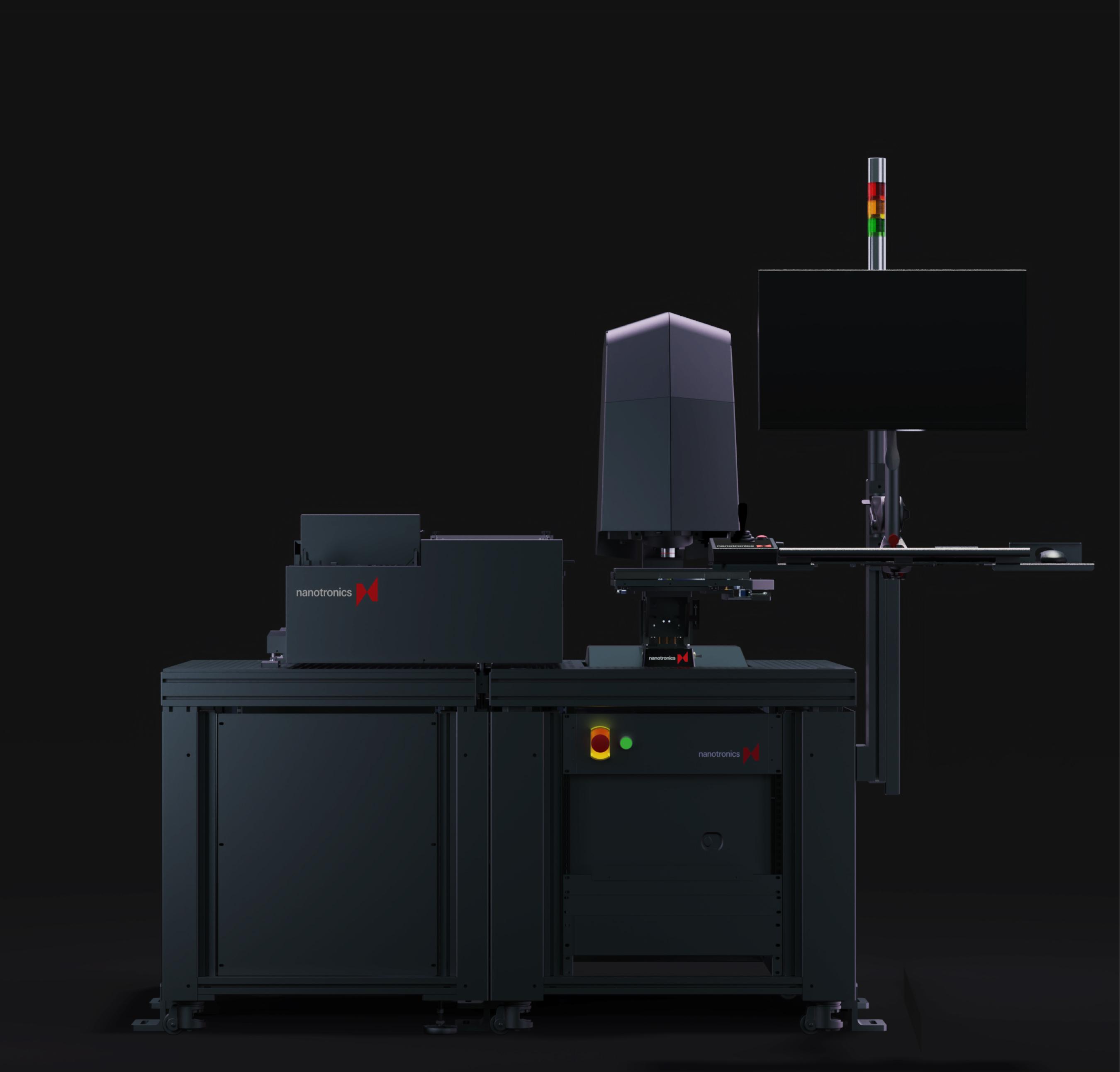
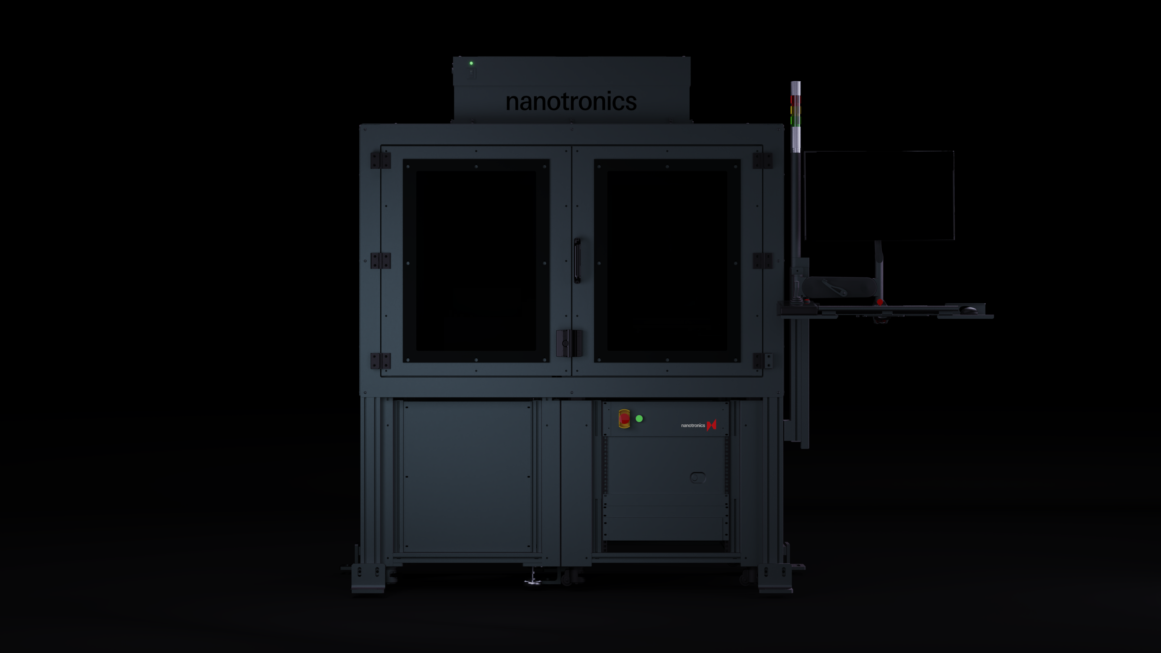
Ideal system for high-volume manufacturing environments. Robotic handling of wafers up to 300 mm or FOUPs to 650 mm.

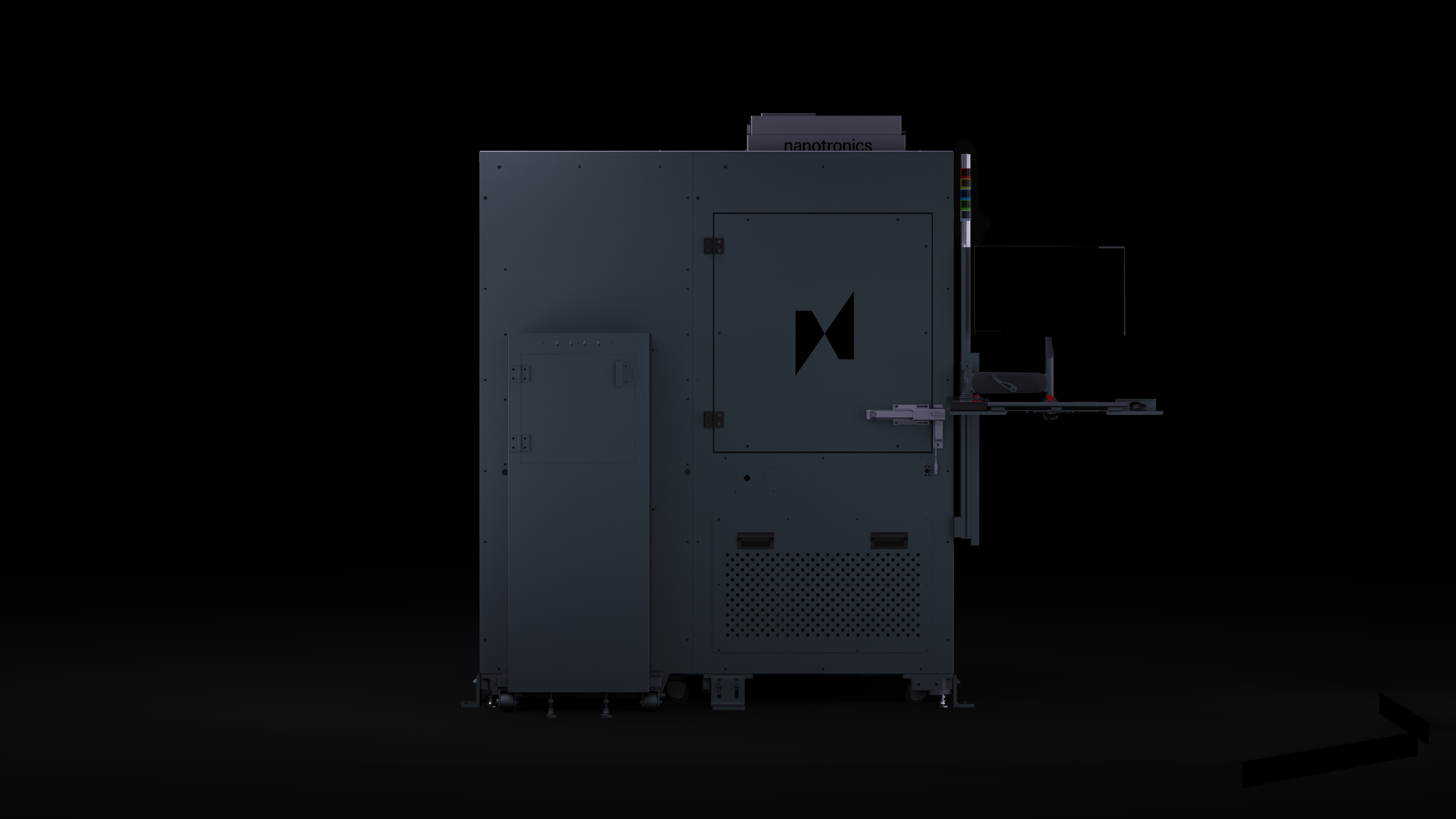
Fully automated high‑volume manufacturing inspection with unprecedented speeds. Enhanced optics, illumination, and robotic motion deliver sub‑micron precision.


Complete solution for compound semiconductor frontend wafer manufacturing. Features UV and IR illumination for the most demanding inspection processes.

A hardware and software tool that will grow with your manufacturing needs


nSpec caters to a wide range of customers. Whether it's R&D, high‑volume manufacturing, semiconductors, healthcare or beyond, our systems offer confidence in consistent quality of output.


nSpec features various levels of automation to maximize production capacity, increase yield, and prevent manufacturing bottlenecks.


nTelligence is able to identify, classify, and assign causality to features of interest. Discover critical defects that otherwise go undetected by the human eye.


nSpec is configurable to meet a range of factory requirements, seamlessly adjusting for dynamic production environments.
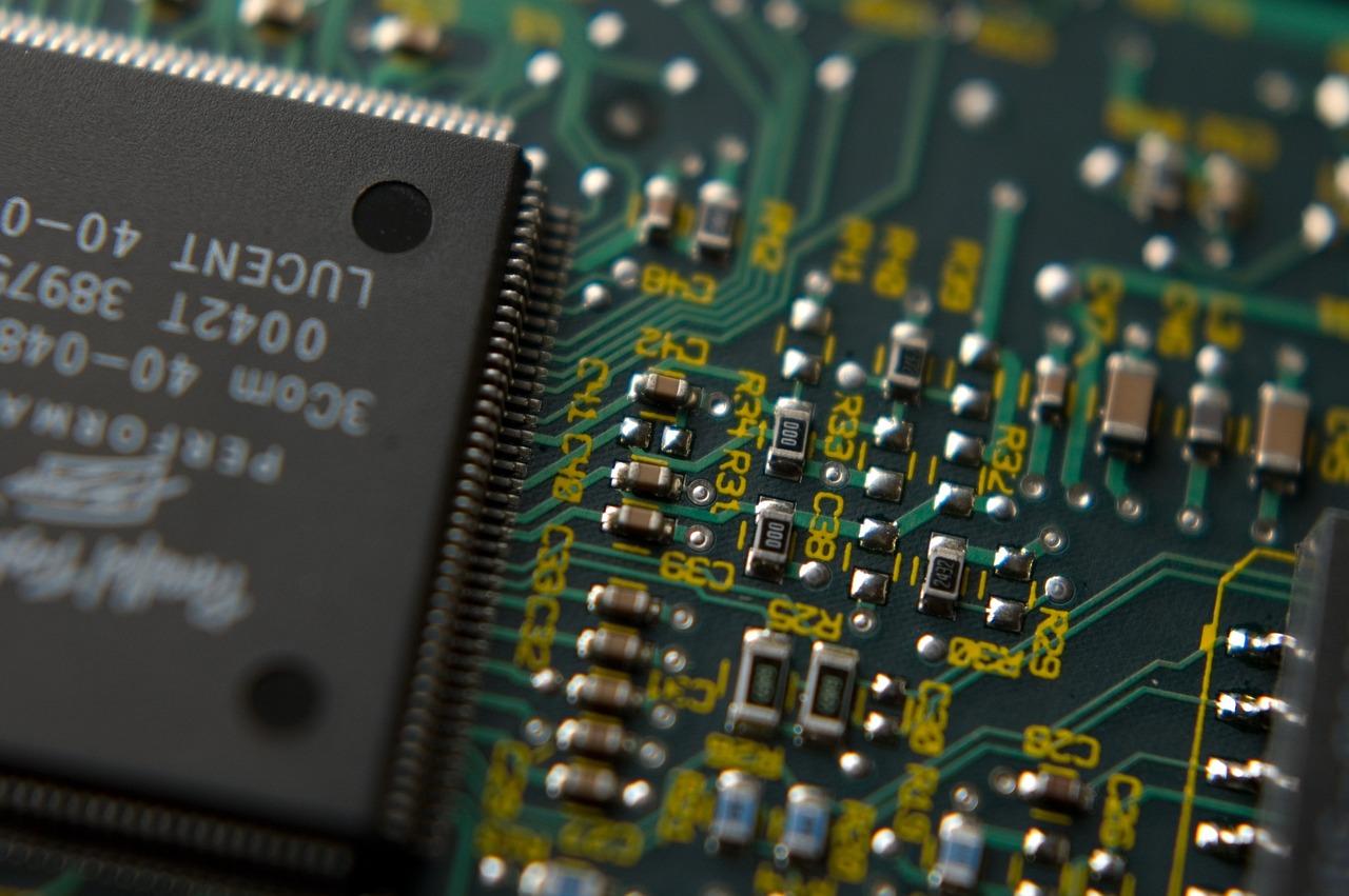
Optical inspection is a way of inspecting defects using inspection tools such as microscopes. It differs from other inspection equipment because of the use of high-quality optics in the inspection equipment. nSpec is Nanotronics name for our line of optical inspection equipment.
AOI stands for Automated Optical Inspection and refers to a quality control process that uses cameras and other optical inspection instruments to identify defects in product manufacturing processes.
Optical inspection instruments are specialized microscopes designed to detect defects on a variety of materials. They can be augmented with software solutions to achieve greater efficiency in defect detection.
Optical inspection systems inspect, identify, and classify defects in different manufacturing environments. They are used in a variety of industries including semiconductor manufacturing and healthcare. Inspectors in these industries use optical inspection equipment because it is a great way to identify defects in a variety of different materials.
Automated Optical Inspection works by using an optical microscope to identify defects in a manufacturing environment. Once the defects are identified, AI powered software helps find the root cause so process engineers fix the problem and minimize manufacturing downtime.
nSpec by Nanotronics offers a variety of optical inspection solutions that are customizable to the varying demands of business needs and budgets. To learn more, fill out the form below.