Case Studies

Destructive vs Non-Destructive Inspection

Scanned image showing micropipe defects in SiC waferScanned image showing micropipe defects in SiC wafer

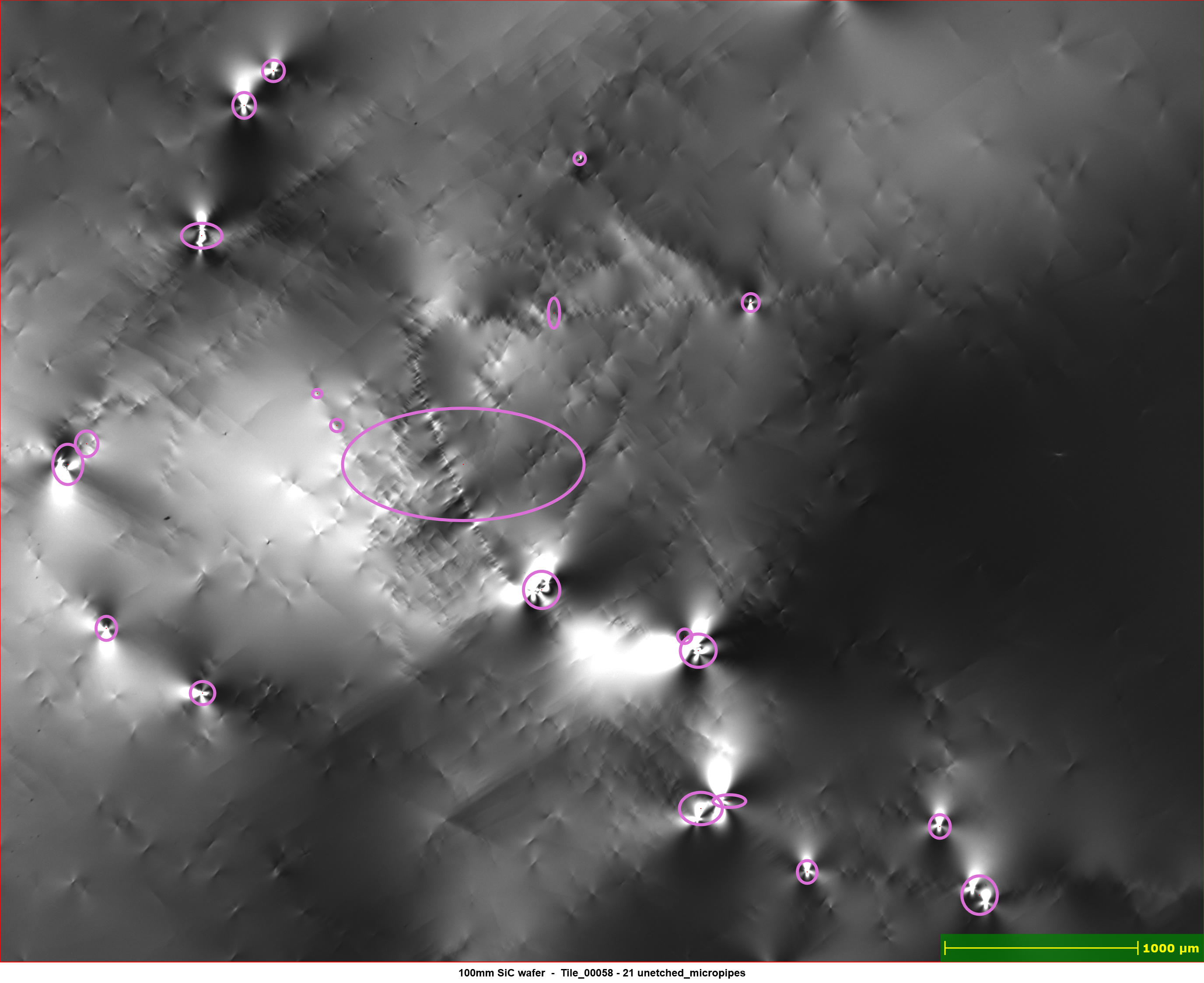
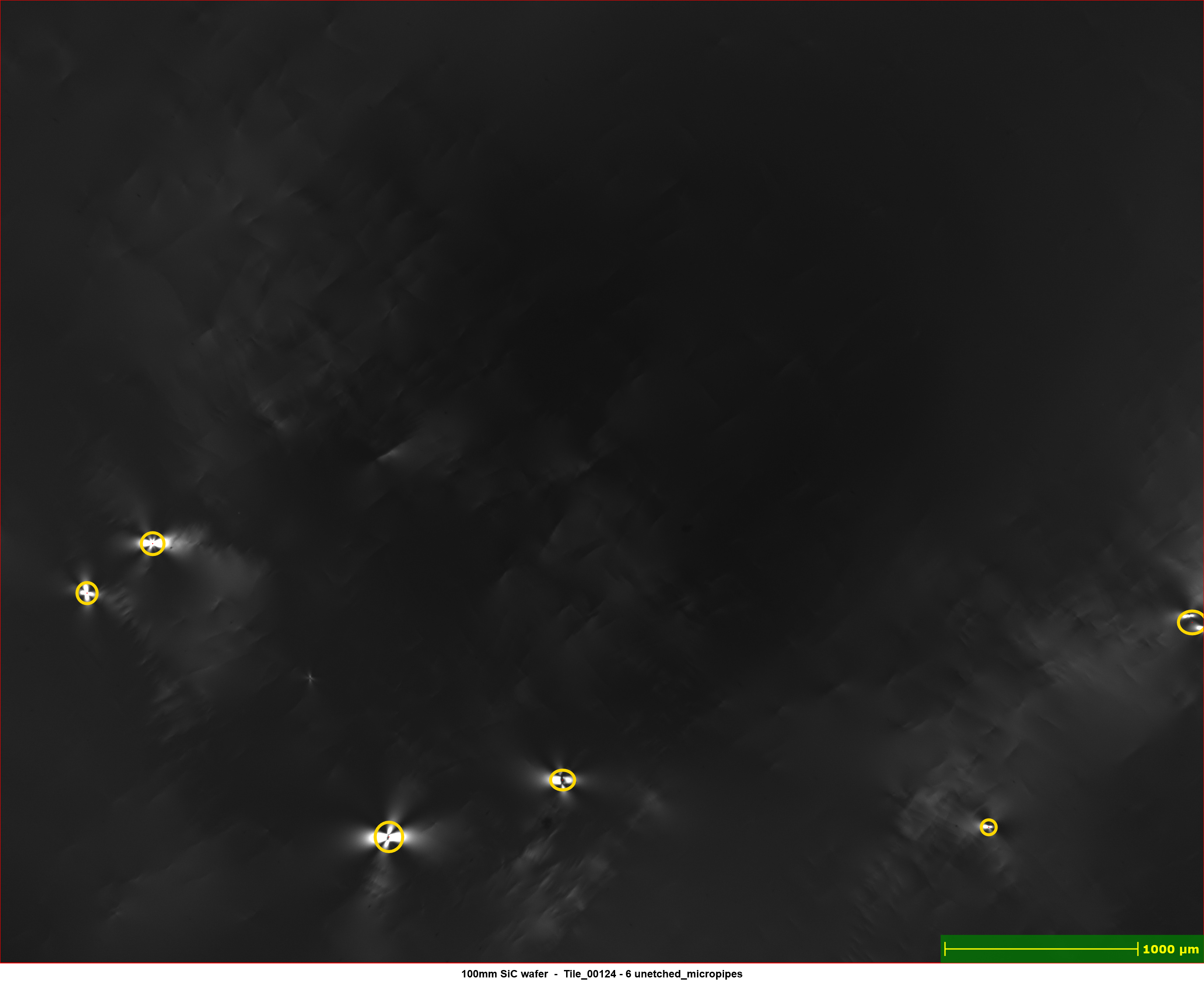
Traditionally, silicon carbide manufacturers identified dislocation-type defects like micropipes using etched wafers—a laborious, destructive process.

Advanced scan of patterned SiC waferAdvanced scan of patterned SiC wafer
Completed scan analysis of patterned SiC wafer

Nanotronics’ patented autofocus algorithms combined with cross-polarized transmitted light and DIC (Differential Interference Contrast) illumination replace such manufacturing processes.

Raw image showing micropipe defects in SiC waferRaw image showing micropipe defects in SiC wafer
Raw image showing micropipe defects in SiC wafer

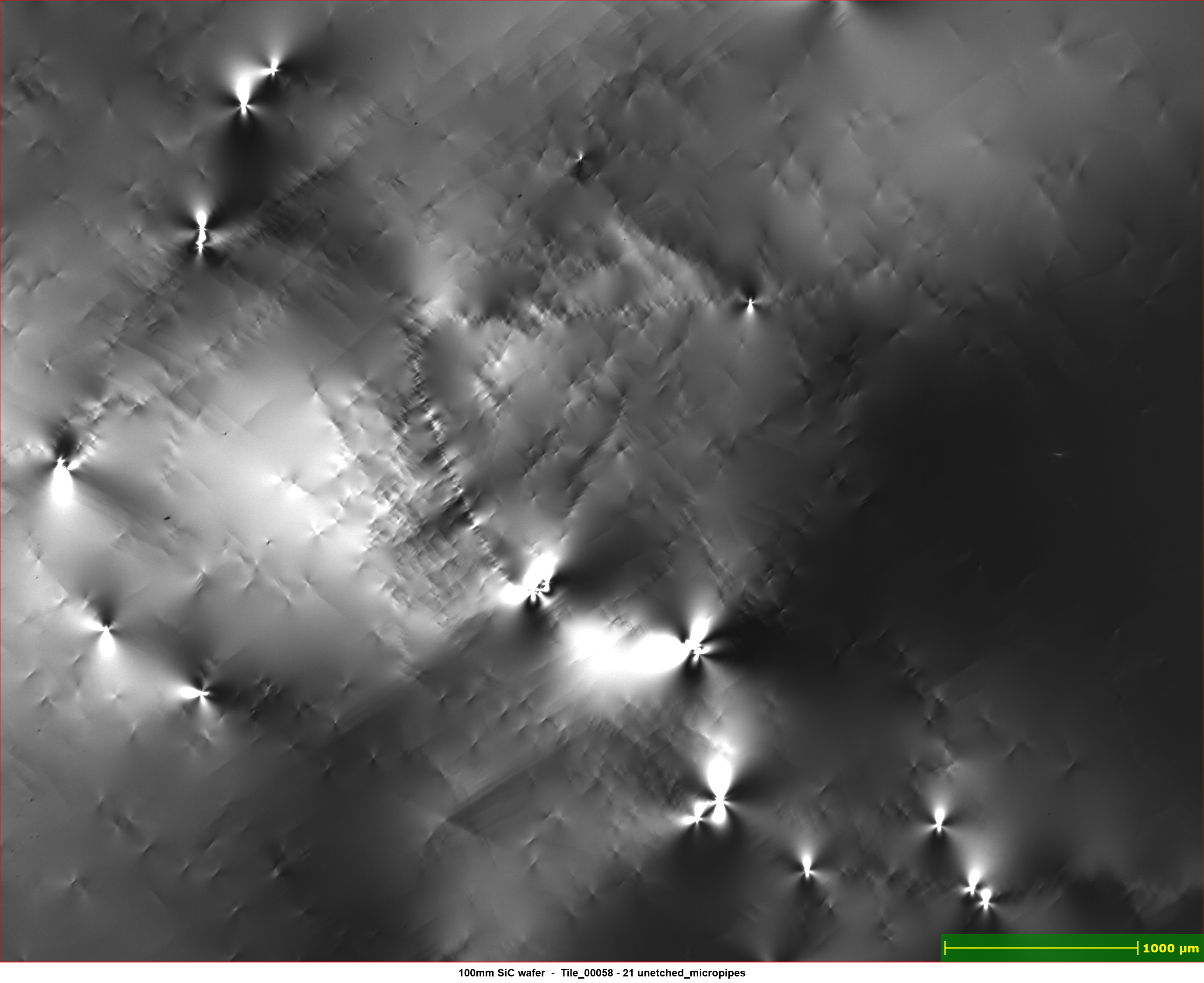
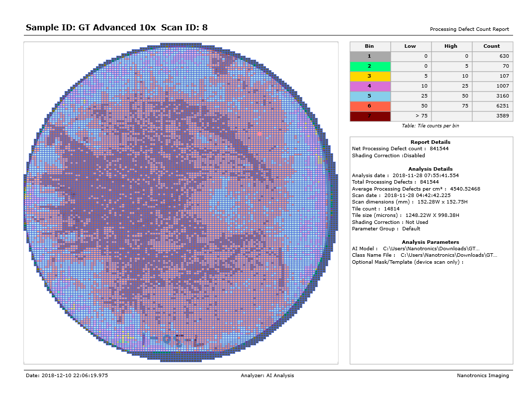
AI classification that detects these subtle, crystallographic substrate defects can be used in-line to provide real-time feedback.

Unetched micropipe defects on 100mm SiC WaferUnetched micropipe defects on 100mm SiC Wafer
Unetched image of micropipe defects on 100mm SiC Wafer

Finally, AI analysis allows the manufacturer to quickly assign causality and differentiate between nuisance and device-killing defects.

Contact Us

Get in touch with one of our industry experts.

Let's talk logistics.

Let’s talk about how Nanotronics can transform your manufacturing process.
Contact Us

Free sample report

Having trouble classifying critical defects? Nanotronics can help.
Get Sample Report