Case Studies

Epi and Substrate Defect Inspection

Defect Map Mosaic of 100mm SiC Epi WaferDefect Map Mosaic of 100mm SiC Epi Wafer
Distant shot of defects on a 100mm SiC Epi WaferDistant shot of defects on a 100mm SiC Epi Wafer
Defects found on a 100mm SiC Epi Wafer

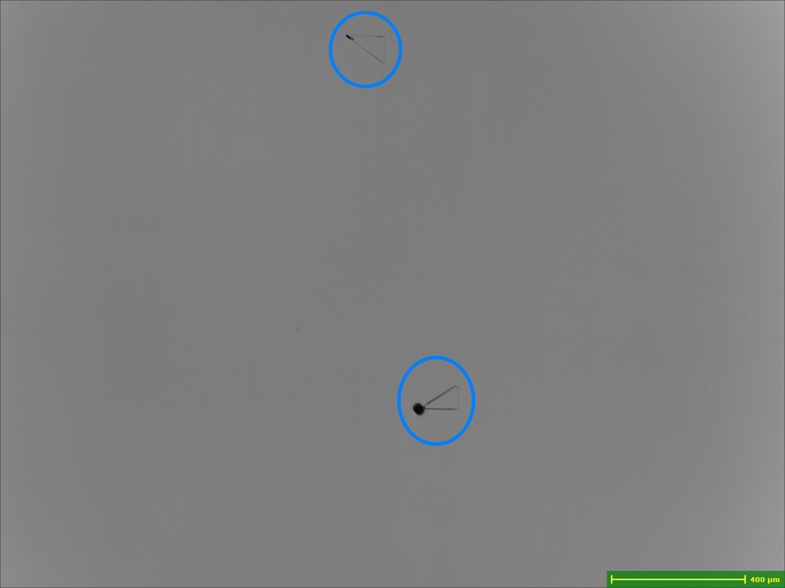
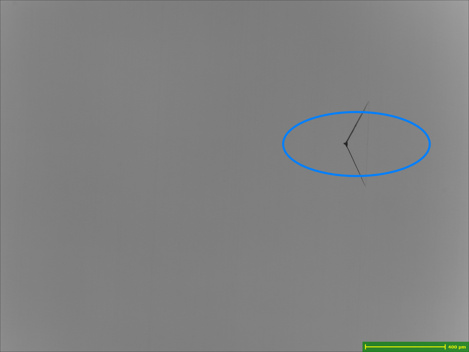
Distinguishing between substrate and epitaxial defects is essential to vertically integrated customers and chief suppliers. The differentiation prevents time-consuming investigations of anomalies.

Classification allows customers to identify at which point a defect was introduced—and take definitive action with devices like the nSpec Macro.

Two defects on a 100mm SiC Epi WaferTwo defects on a 100mm SiC Epi Wafer
Two defects on a 100mm Sic Epi Wafer Tile
Close up of defect on a 100mm SiC Epi WaferClose up of defect on a 100mm SiC Epi Wafer
Close up of defect on a 100mm SiC Epi Wafer

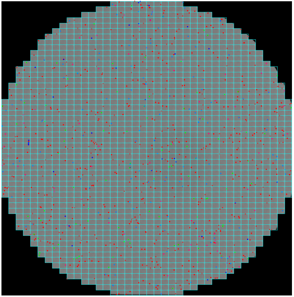
nSpec enables users to create new classifications as the need arises during manufacturing. This gives customers complete flexibility as they develop new materials or change processes.

Contact Us

Get in touch with one of our industry experts.

Let's talk logistics.

Let’s talk about how Nanotronics can transform your manufacturing process.
Contact Us

Free sample report

Having trouble classifying critical defects? Nanotronics can help.
Get Sample Report