
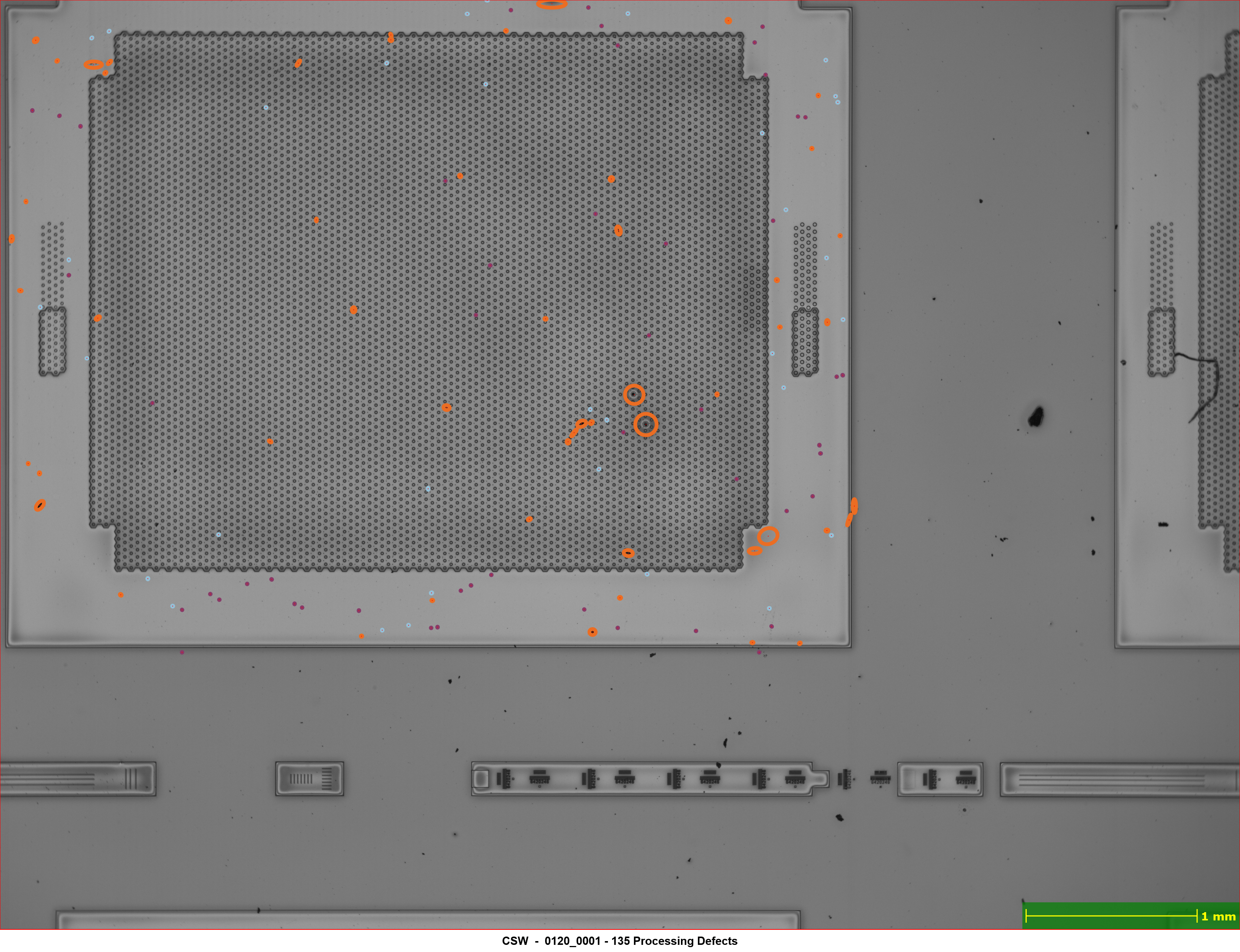
With nSpec, inspection becomes comprehensive throughout the lithography/patterned wafer manufacturing process.
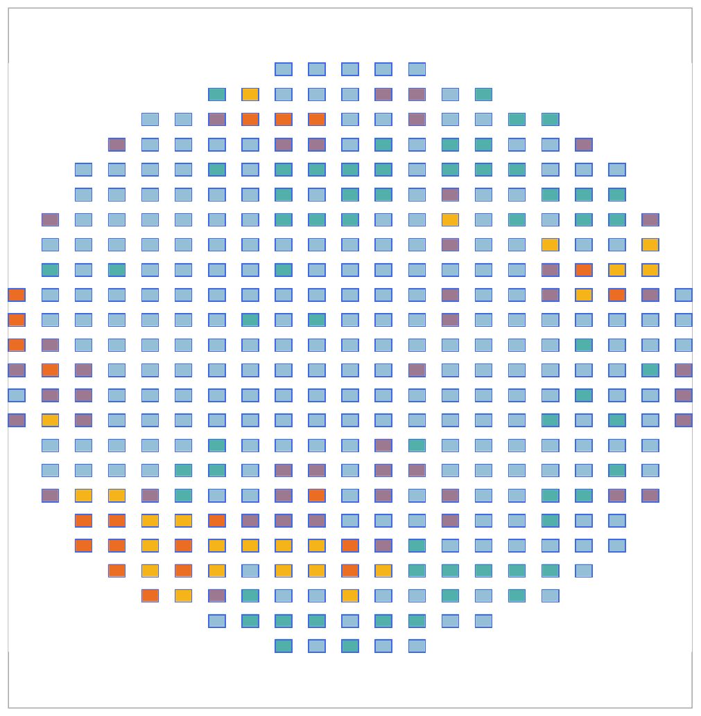
nSpec Macro uses a golden template–based method to capture subtle defects where tolerance is very low, while limiting false positives in regions that have a higher level of variation or noise. Yield-loss data can help flag systematic issues.

Defect information associated with each die can be sent to back-end processing, and dies can be excluded in subsequent steps of manufacturing, reducing needless expenses.
nSpec can be strategically placed in each processing bay due to its low cost of ownership and small footprint, eliminating the need to move wafers to a central inspection bay.

nSpec handles the most complex use cases ranging from numerous small devices within a single field of view to large devices comprised of multiple fields of view, as well as non-repeating devices or even/odd device patterns.