
Wafer inspection refers to the methods, tools, and technologies used to detect physical defects and pattern irregularities on semiconductor wafers. Since 2025, these tools include both electron and optical beam systems, and in an industry where even the tiniest defect can result in major device failures, wafer inspection systems ensure quality, efficiency, and cost-effectiveness of semiconductor products.
In this article we will explore:
- What wafer inspection is
- How wafer inspection works
- How businesses can use wafer inspection strategies to optimize manufacturing
- Wafer inspection FAQ
What is Wafer Inspection?
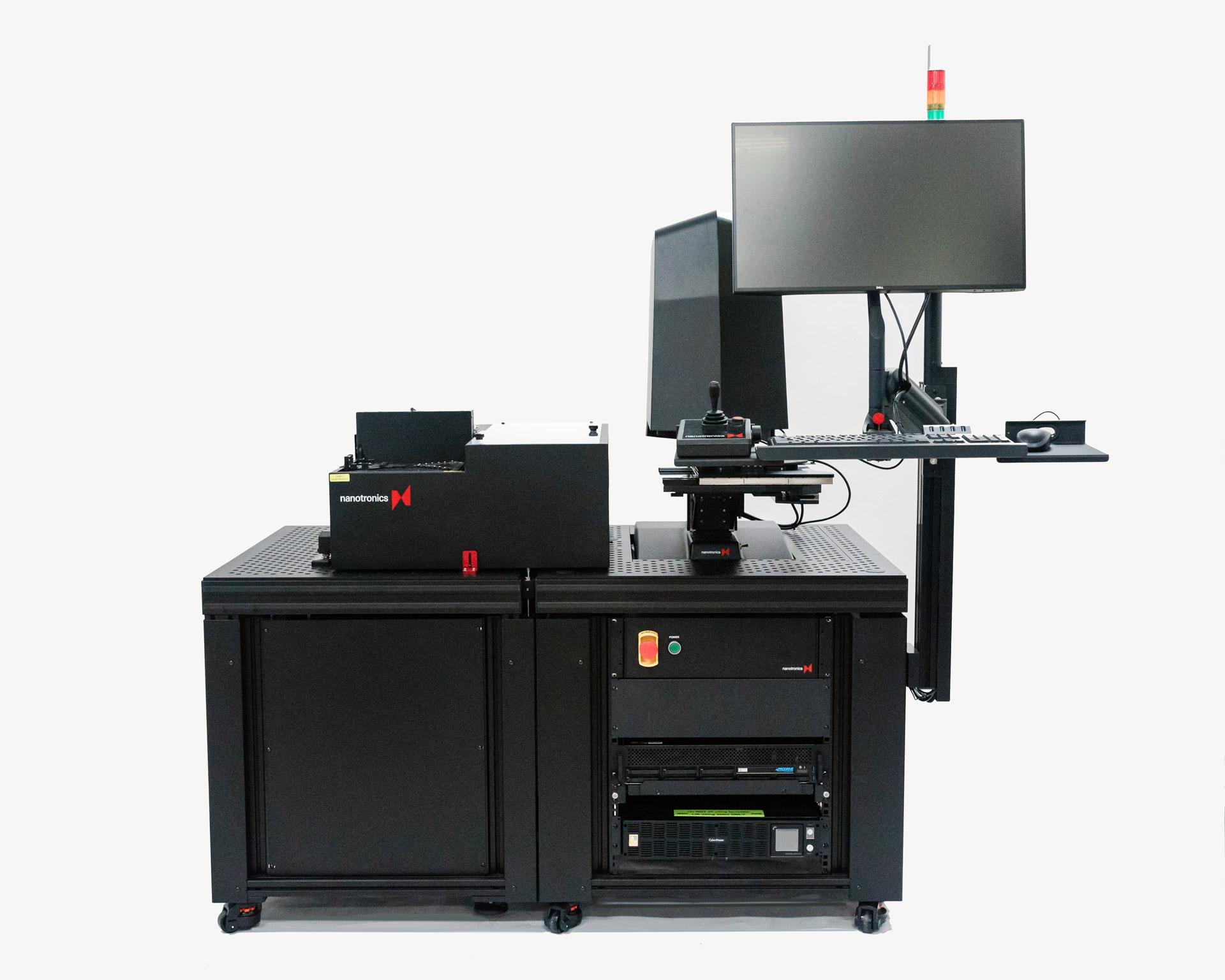
Wafer inspection involves examining semiconductor wafers for defects that could affect the functionality of the final electronic devices. These inspections are crucial for products ranging from smartphones to AI systems, making inspection accuracy essential for industries worldwide. Process engineers use a combination of advanced optical systems, electron beams, and sophisticated algorithms to identify defects that would be impossible to detect with the naked eye, while obtaining precise position coordinates of any anomalies found.
How does Wafer Inspection Work?
Wafer inspection is conducted on both patterned process wafers and bare wafers, with each requiring specific system configurations. There are numerous inspection points throughout semiconductor manufacturing. When these points are functioning optimally, they create an effective quality control system. However, due to the nanometer-scale precision required in modern semiconductor fabrication, even minor errors can lead to significant issues. Common challenges identified include:
- Random defects from particles adhering to wafer surfaces.
- Systematic defects resulting from mask and exposure process conditions.
- Light reflection interference that affects detection accuracy.
- Throughput limitations in high volume manufacturing.
- Balancing sensitivity with false detection rates.
These challenges can lead to substantial yield losses, impacting factory efficiency and resulting in considerable material and financial waste.
FAQ about Wafer Inspection Systems
What is wafer inspection?
Wafer inspection is a critical process in the semiconductor manufacturing industry, designed to identify and analyze defects on semiconductor wafers. This method involves using advanced inspection tools and systems to examine the wafer surface for any irregularities that could affect the performance of the final electronic devices. By employing techniques such as optical and electron beam inspection, manufacturers can detect defects at various stages of production, ensuring high-quality output. The inspection process is essential for maintaining the integrity of high volume manufacturing, as it helps in detecting and addressing potential issues early on, thereby reducing yield losses and improving overall efficiency. Optical inspection is commonly used for wafer inspection and you can learn more about this on our deep dive linked here.
What is a wafer handling system?
A wafer handling system is an integral component of the semiconductor manufacturing process, responsible for the safe and precise movement of wafers through various stages of production. These systems are designed to handle wafers delicately to prevent damage or contamination, using robotic arms and automated mechanisms. By ensuring the accurate positioning and transportation of wafers, handling systems play a crucial role in maintaining the quality and consistency of semiconductor devices. They support the inspection process by allowing wafers to be presented to inspection tools with precision and reliability.
What is the wafer coordinate system?
The wafer coordinate system is a framework used to map the exact position of defects or features on a semiconductor wafer. This system assigns precise X and Y coordinates to locations on the wafer, enabling manufacturers to accurately identify and track defects throughout the production process. By utilizing the wafer coordinate system, engineers can better analyze defect patterns and implement targeted corrective actions, enhancing the overall quality of semiconductor products. This system is vital for process monitoring and development, as it provides a consistent reference for evaluating wafer inspection results.
What is wafer fault detection?
Wafer fault detection is the process of identifying defects or anomalies on semiconductor wafers that could lead to device failures. This involves using sophisticated inspection tools to detect defects such as particles, scratches, or pattern deviations on the wafer surface. By employing high sensitivity inspection systems, manufacturers can find defects that are not visible to the naked eye, ensuring that only wafers meeting stringent quality standards proceed to the next stages of production. Effective fault detection is crucial for preventing yield losses and maintaining the reliability of semiconductor devices in high volume manufacturing environments.
The Bottom Line
Wafer inspection is complex, but with the right inspection techniques, companies can reduce defects, increase yield, and improve overall semiconductor quality. Whether it's optical inspection, high-resolution bright field imaging, scattered light detection with dark field systems, or something else, these techniques ensure that every wafer meets the highest standards before moving to the next manufacturing stage.
Unsure what inspection solutions are right for your semiconductor manufacturing line? Click here to schedule a call with one of our experts.